Table of Contents (click to expand)
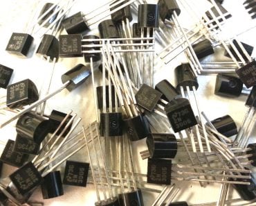
A Zener diode is a special type of diode that allows current to flow in both directions. Zener diodes aren’t constructed the way conventional diodes are: they are excessively doped to reduce the depletion width. Lower voltage also makes the diode more robust, as it averts the danger of being damaged irrevocably.
Recommended Video for you:
What Is Zener Diode?
A Zener diode is a special type of diode that lies at the heart of voltage regulators and circuits generating the reference voltage for a differential amplifier. The USP of a Zener diode is that it conducts current in both directions, but what is so unique or special about that?
The Diode
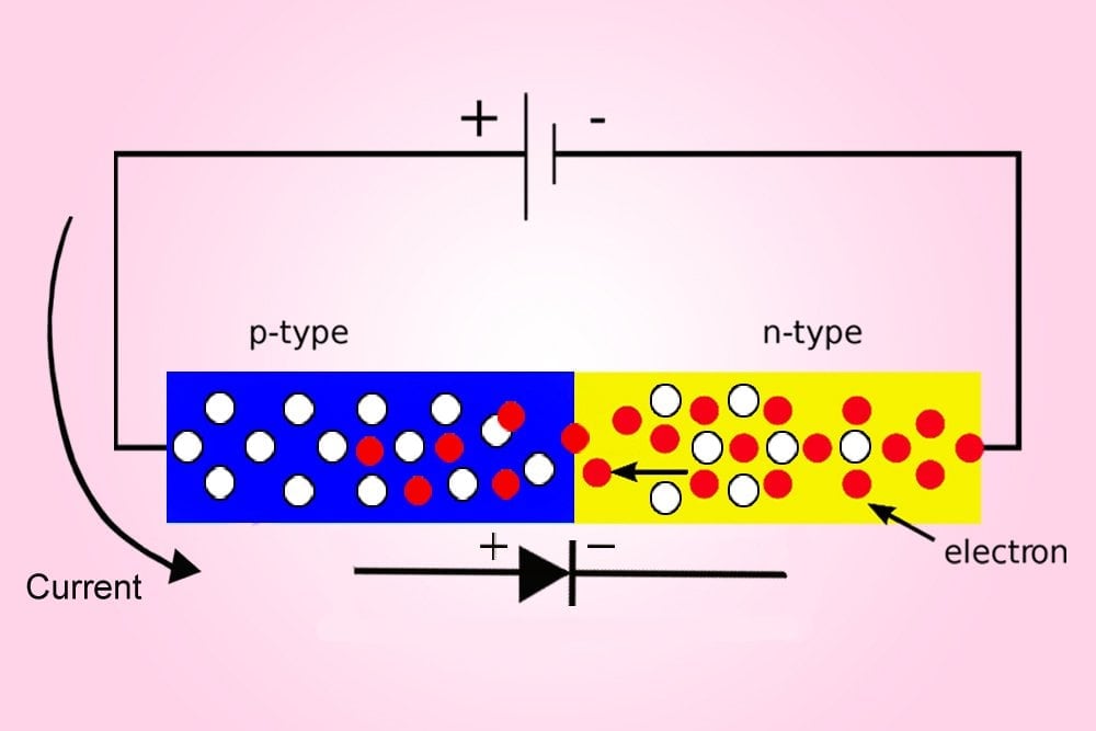
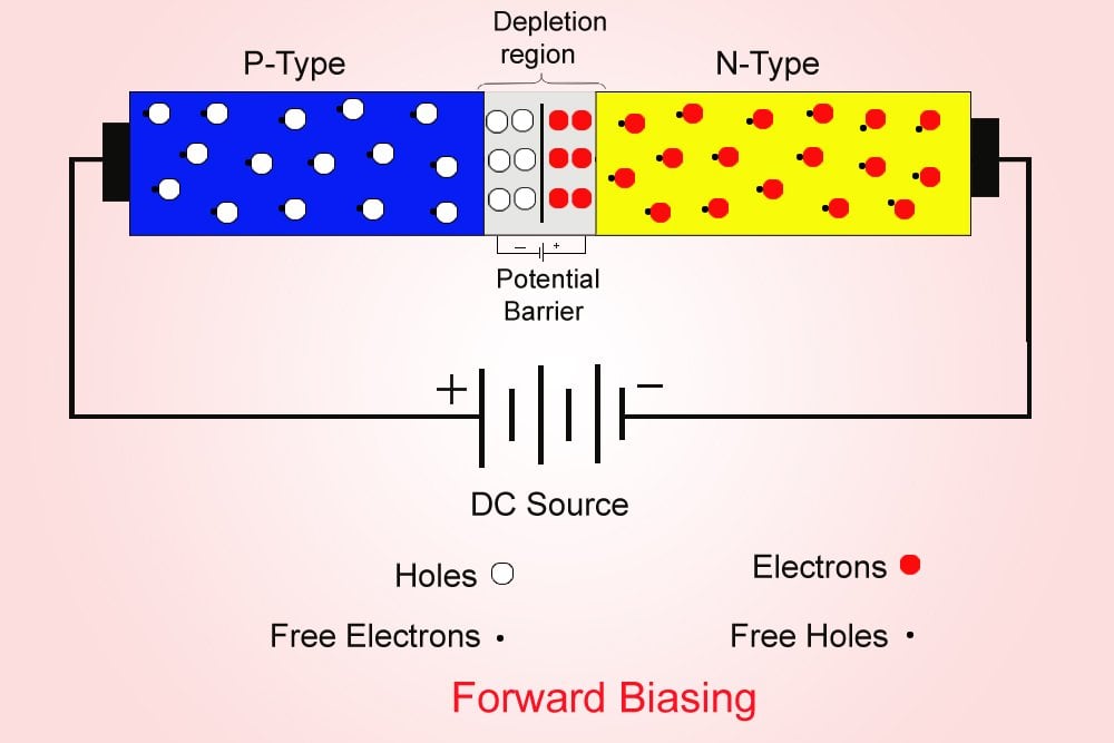
A diode is basically two slabs of semiconductors glued to each other. However, the semiconductors differ in their properties: one is electron-impoverished, or exhibits an excess of positive charges or holes, while the other is suffused with electrons and therefore exhibits an excess of negative charges. Together, they constitute what is called a PN Junction.
The fundamental purpose of a diode, unlike a resistor, is to allow current to flow in only a single direction. Current through a diode will only flow when it is forward biased or when its positive semiconductor, or anode, is connected to the positive terminal of the battery, while its negative semiconductor, or cathode, is connected to the negative terminal of the battery. On the other hand, the current is stifled when the diode is reverse biased, or when its terminals are cross-connected.
A diode only conducts when forward biased.
Forward Bias
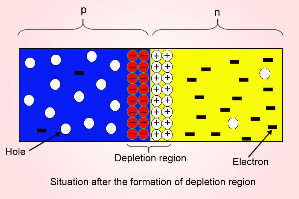
Initially, when the two slabs are combined, some electrons from the n-type semiconductor will be lured by the p-type semiconductor and will diffuse across the junction to the other side. Similarly, the holes, lured by the n-type semiconductor, will squeeze their way to the other side. This diffusion will deplete the holes in the p-type semiconductor and the electrons in the n-type semiconductor. The two narrow regions between the junction depleted of charges will together form the depletion region.
Being formed due to a flow of charges, it manifests a potential difference. Let’s say that its value is some V(x) volts. Now, because the electrons flowed from right to left, by convention, current flowed from left to right, so the p-semiconductor represents a positive terminal, while the n-type semiconductor represents a negative terminal.
When a diode is forward biased with a voltage V, the depletion region voltage V(x) will oppose it. This is because they are aligned opposite to each other. The two voltages supplying currents in the opposite directions are basically arm wrestling. In this way, the depletion region acts as a barrier to the flow of current.
However, as the voltage V increases, its hand eventually overpowers V(x)’s hand and pins it to the ground. A large voltage overcomes the barrier voltage, as the large positive voltage will pull out the electrons from the depletion region and the large negative voltage will pull out the holes from the depletion region. Further increasing the voltage will also pull the electrons and holes from the semiconductors. The depletion region width, W, will gradually decrease until it completely fades away, allowing the diode to draw a current.
Reverse Bias
On the other hand, when the diode is reverse biased or, to remind those who weren’t paying attention, when the positive terminal of the battery is connected to the n-type semiconductor and the negative terminal is connected to the p-type semiconductor, the two voltages add up. This is because they are now aligned in the same direction.
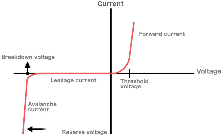
This is analogous to a cue ball hitting an 8-ball that was already moving away from it. However, this actually makes the diode unyielding. The negative terminal attracts holes from the p-type semiconductor and the positive terminal attracts electrons from the n-type semiconductor, thereby widening the depletion region. The barrier is now strengthened! A further increase in the reverse bias voltage will further increase the width (W) of the depletion region. Still, because charges, however meager, drift from the junction to the terminals, the diode draws a very small current – a leakage current – in the range of microamperes.
An electric field is a function of width, so for a large reverse bias voltage, and therefore depletion region width, the electric field is enormous. The leakage current flows until the applied voltage reaches a certain high value called the breakdown voltage, beyond which the ions go haywire.
At the breakdown voltage, the electric field grows so intense that the ions vigorously scamper and collide with the diode’s atoms, knocking out more and more ions. The diode can no longer bear the pressure and the floodgates are forced open. The result is an avalanche breakdown, a sudden and astounding increase in current. The diode is heated so greatly that subjecting it to a voltage greater than the breakdown voltage damages it irrevocably. This is why conventional diodes aren’t operated in reverse bias.
Enter the Zener diode.
Also Read: What Are Semiconductors? And How Do They Work?
The Zener Effect
The Zener diode is a diode that is employed specifically to operate in reverse bias. The diode doesn’t suffer from an avalanche breakdown, but a slightly different kind of breakdown that is now called the Zener breakdown.
One can infer from the graph that, following the avalanche breakdown, even a small increase in voltage would cause the diode to draw a huge amount of current, that is, the diode still exhibits variation. However, a diode that is “doped” adroitly will draw a huge current, but will not exhibit any variation: the voltage across its terminals will remain the same. This is the working principle of a Zener diode. The diode is named after Clarence Melvin Zener, the man who discovered this peculiar effect.
A Zener diode typically suffers a breakdown at a marginally lower voltage than a conventional diode does. This voltage is called the Zener voltage. The diode functions just like any PN diode while forward biased, but its sharp breakdown or its stark indifference, the fact that its voltage remains absolutely constant, despite a spike in current when suffering a breakdown, is what makes it so useful.
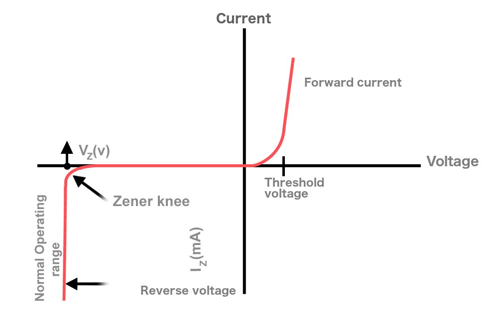
The voltage across circuits connected in parallel are equal, which means that the voltage across a circuit will remain constant or equal to the breakdown voltage of a Zener diode connected in parallel with it, even though the current within it might unexpectedly fluctuate. To limit the tremendous current, a resistor is employed in series. In this way, a Zener diode can be used to regulate voltage.
Any device’s properties ultimately come down to its composition. Zener diodes aren’t constructed the way conventional diodes are: they are excessively doped to reduce the depletion width. The result is a weaker barrier, which is why the breakdown voltage of a Zener diode is lower than the breakdown voltage of a simple diode. A lower voltage also makes the diode more robust, as it averts the danger of being excessively heated and therefore being irrevocably damaged.
Also Read: What Is Internal Resistance? How A Battery Works?